
AT&T Bell Labs (~1990-2)


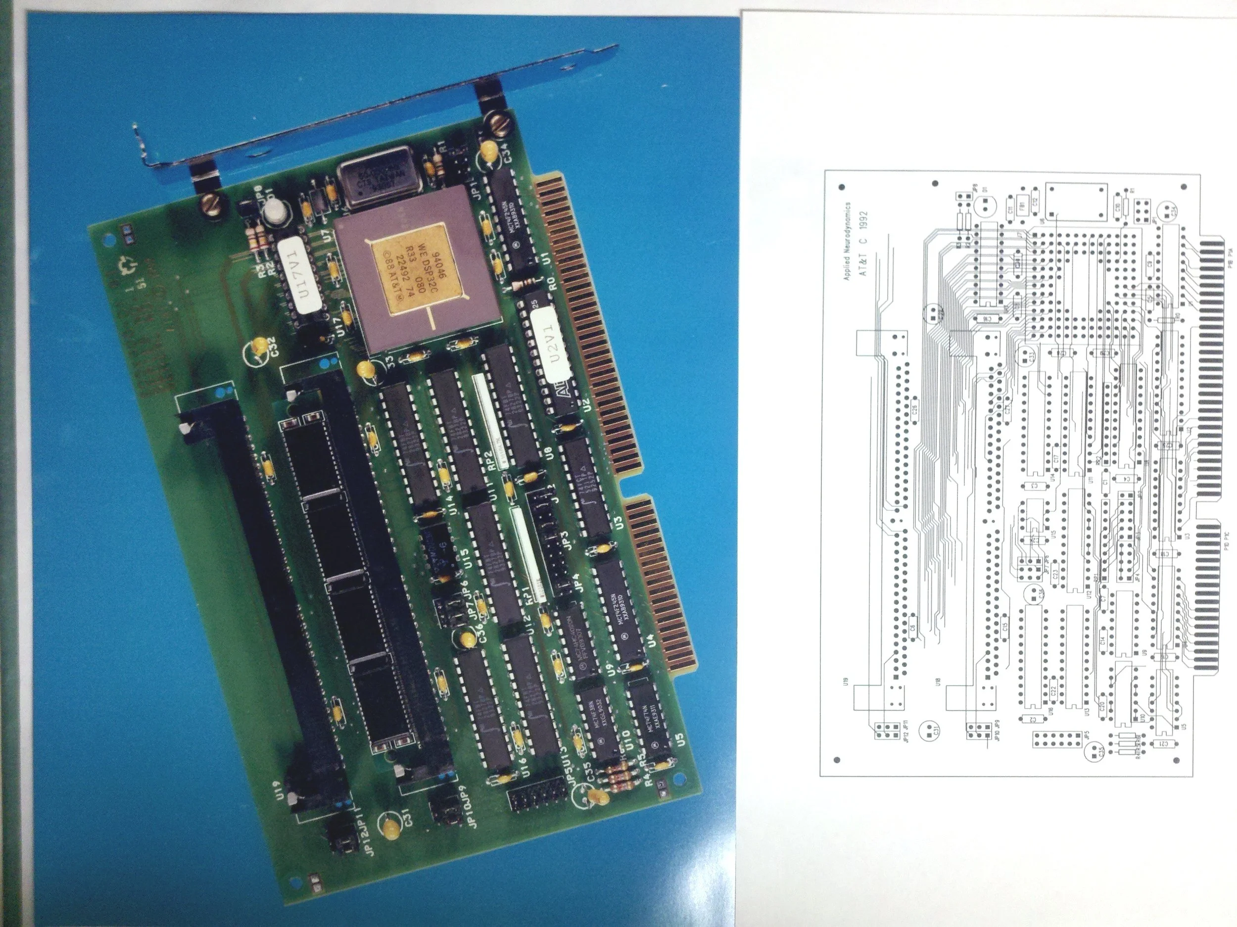
AT&T Bell Labs had a strong neural network group in the early 1990’s including Graf, Sackinger, Boser, Jackel, and Yan Le Cun together designing chips and algorithms where I landed some contract work. The top two boards were for Hans Peter Graf’s Net32K analog chip. Both had a DSP32C processor and RAM. The top left (1st) one is a multiwire board in which you might be able to see the embedded wire if you zoom in. Top right (2nd) is the layout for the PCB version built to host the NET32K that followed. The bottom left (3rd) board has the ANNA, Analog Neural Network ALU, chip along with a DSP32C in the PC AT (ISA) bus form factor. The 4th on the bottom right is just a compact DSP32C for use in ATM machines doing check scanning. I made many of these for AT&T. Most of these boards used SRAM to minimize DSP wait states. At this stage in my career, I had been doing all the schematics and most all IC placements with customer guidance. Then I would turn the job over to a real PCB designer to manually route the high-speed signals with me sitting with them and advising. Then we would let the design be completed with an autorouter overnight with post route cleanup. This allowed for pretty fast board deliveries. Once in a while, there was an error on my part as was the case for the last board below. This was to be a High-Speed ANNA board using 4 Xilinx FPGAs with me doing the schematics and board design, and AT&T doing the FPGA programming based on their proprietary algorithm. I misunderstood and did not get the signals right between the FPGAs, and I was running late. I do not know if it was ever able to be used. )-: My bad. :-(
