Oxford University, Rodney Douglas Lab which became
ETH Institute for Neuroinformatics (~1994-5)
This design is called the Silicon Cortex Board and was one of my greatest challenges. As I often say, I worked for two years crammed into one year for one half of one year’s pay to do this. Nothing was allowed to interfere with this project. I had hoped it would result is many publications. This design was to enable a project testing a new Silicon Cortex chip inspired by Carver Mead’s approach to NME and designed by the late Misha Mahowald who became one of the NME field’s greatest losses before her project could complete. She worked with Rodney Douglas to found INI at ETH, Zurich. People seemed more interested in carrying forward Misha’s work on silicon retinas rather than the silicon cortex chip (until maybe recenly), and I don’t believe anyone ever explored what all this board was capable of.
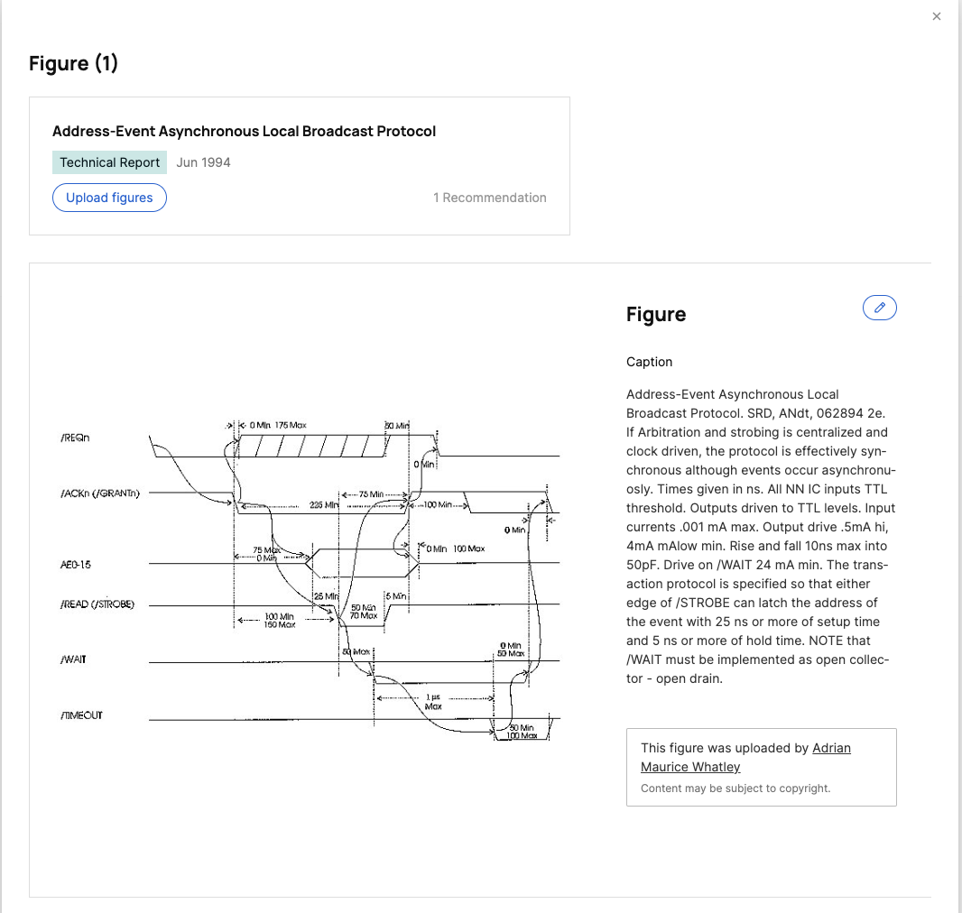
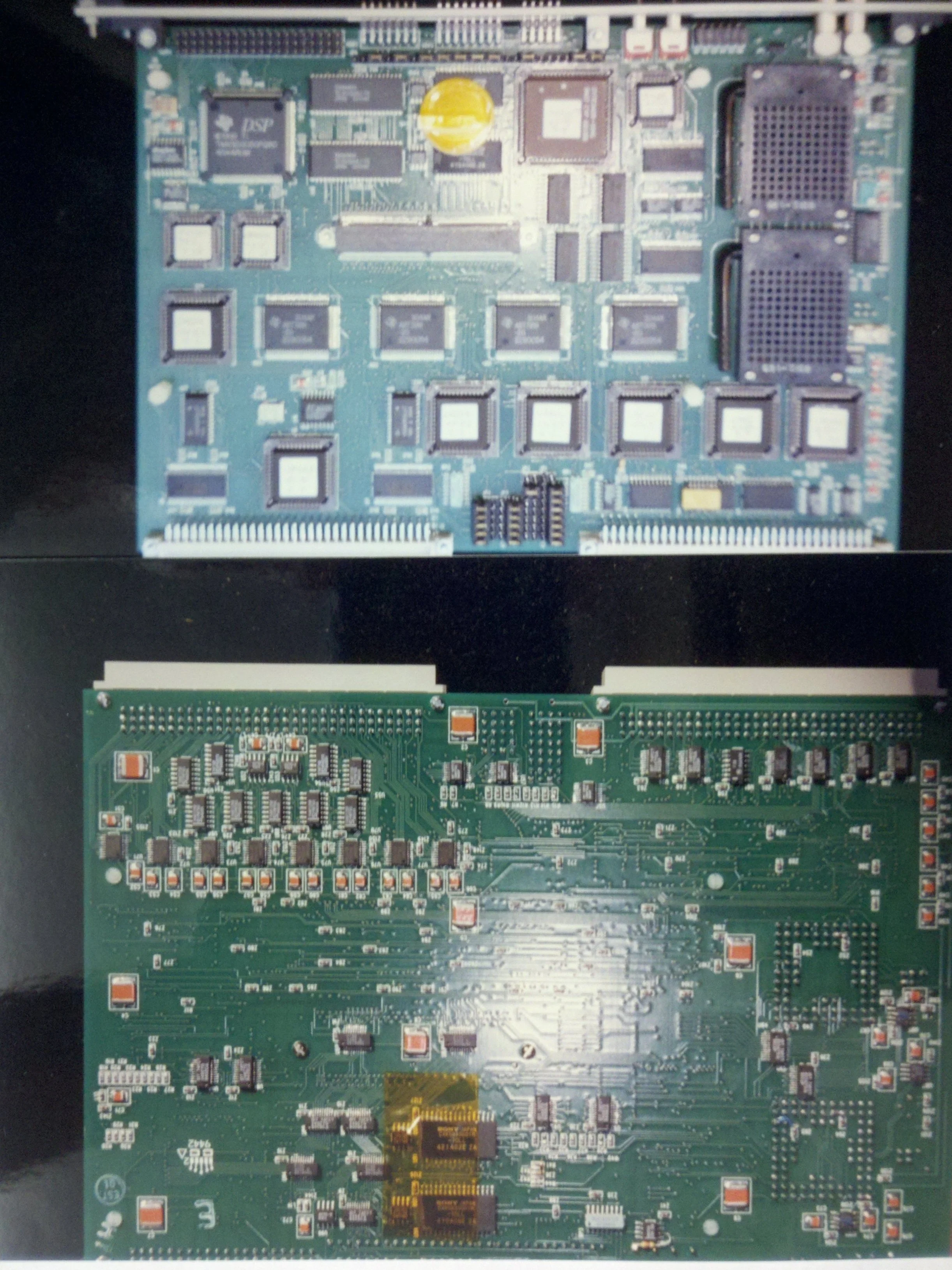
Some things to note: I delivered 5 of these overseas with some export hassles I never encountered before. Each could hold two SCX on the main board, and several more on a mezzanine board that would fit the large center connector. This was double-sided surface mount with a vengeance with lots of analog and lots of high-speed digital close together, but it still fit in a single-wide VME slot. There were 11 Cypress Semiconductor complex PLDs on board that I programmed with VHDL. One of these was a state machine address event bus arbiter I developed after putting together an actual timing diagram (see below) that the Oxford group could sign-off on as meeting their definition of AER. Two were for AER Domain busses that went through the VME AUX connector. I developed a variant of NUBUS arbitration with fairness that allowed arbitration to overlap bus transmission so that multiple masters in different slots, up to 8, could send events in rapid succession with no wait states between. Domain speed was tested over ribbon cable at 20 MHz. Bus termination position was jumper specified. Urgency of delivery prevented completion of the domain bus event filter logic that would allow a board to decide which events to allow in. The onboard CPU was a 40MHz TMS320C50. There was battery-backed SRAM for weight and state parameters which explains the teflon tape on top and bottom to prevent shorts during handling.
Had I just done the logic design and placement as usual, that would have been hard enough. However, the funding was minuscule for something this complex and for the parts cost. I had a mortgage and mouths to feed and limited savings buffer. This would have been a difficult mixed analog layout for any PCB designer, and easy to get careless. So I decided to save a little and do all the layout myself for the first time, all manual, no autorouting. So not counting the preliminary handshaking and after fab publication, the bulk of the design, build and test was done in about one year. I did the assembly and all soldering myself by hand too. We went from getting acquainted at an Idyliwild Workshop in 1993, specifying it before the Telluride Neuromorphic Workshop in 1994 to delivering it before the Telluride Workshop 1995. Adrian Whatley did all the software drivers for the board and helped nail down board specs as my primary liaison with the Oxford team as we went along.
There was discussion of doing a funded follow-on design, but where there was money in hand, there was foot-dragging to release it. Where there were collaboration opportunities, people balked at signing an NDA. When ONR funding did arrive it came with unexpected rivalries to deal with that ignored the personal effort just completed. So I moved on and SCX became a museum piece. I know of only one publication about this SCX system that resulted thanks to Douglas and Whatley, but that one does seem to be often cited.