UCSD (2006-2022)
There have been several designs completed for UCSD over the last two decades. Some are neuromorphic, and others are for BMI, brain-machine interfaces, such as EEG.
Most of my UCSD work was done in Prof. Cauwenberghs’ Integrated Systems Neurogengineering Lab, except for a couple small designs done in Prof. Steve Swanson’s Nonvolative Systems Lab in CSE, or one year-long software project in Eric Halgren’s Multimodal Imaging lab. There were multiple service breaks or time reductions due to funding cuts. But like a true glutton, I kept coming back for more until retirement. I continued mainly so that I could stay closer to the neuro and cogsci research and scratch that itch I came down with as an undergrad when I studied Donald Hebb’s classic! His ideas about learning that we discussed in a graduate seminar there really made sense.

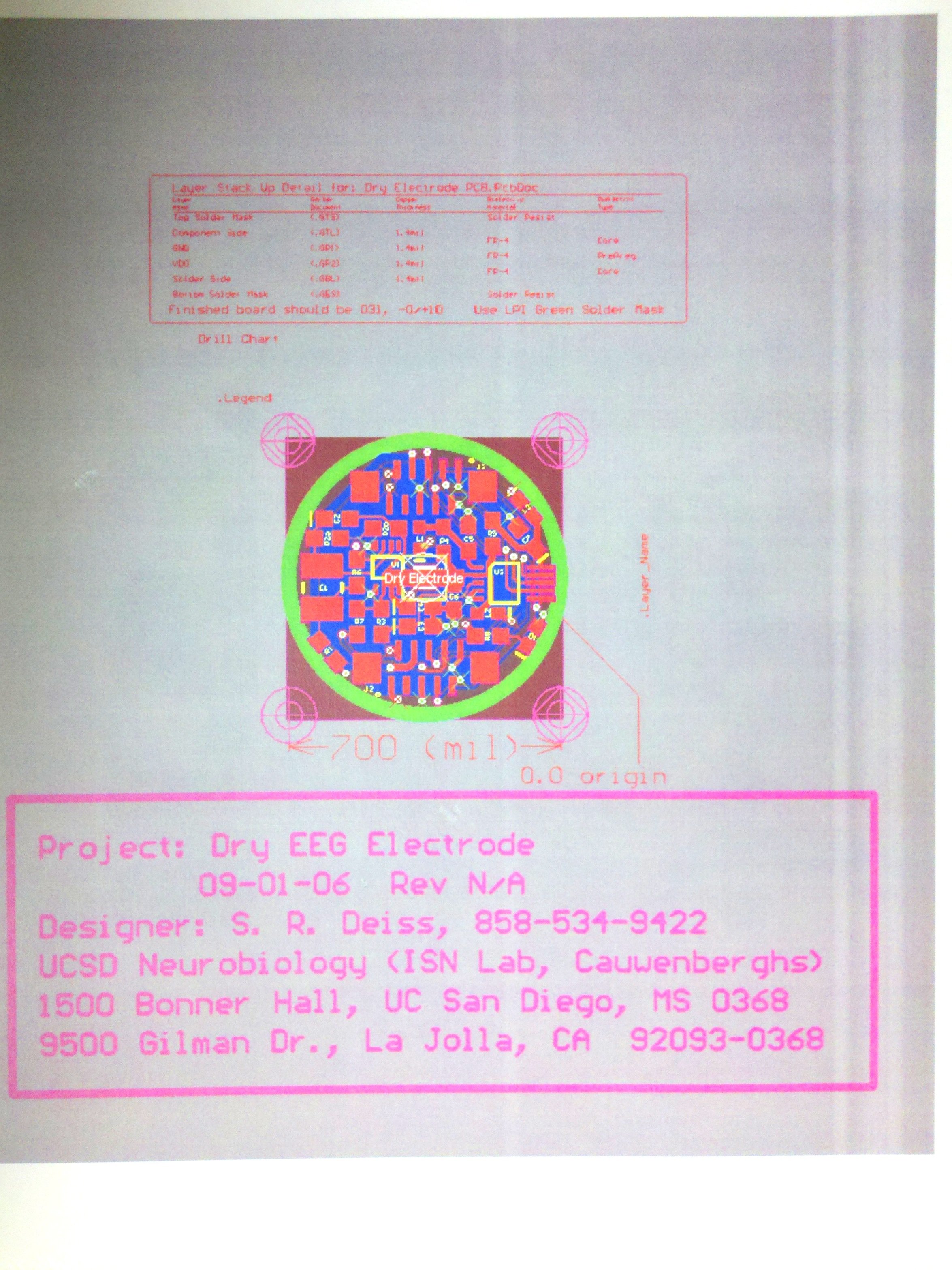
2007: Aftert helping Gert build his first engineering lab in Bonner Hall, we got busy doing design. The above was a quarter ($) sized circuit that was AFAIK the first to capture EEG without requiring gel coupling. Dr. Tom Sullivan was the architect with Gert Cauwenberghs’ guidance. I did the schematics, layout, fab, assembly . . .
You can read more about this design here.


2008: Above was a project intended for connection to a Khepera mobile Robot. The robot has two wheels, motors, and motor control to which one can send drive commands to move it around. These two boards are about the width of a tea cup plate, the diameter of the Khepera. One can design add-on circuits like these with computers, WiFi connections, vision sensors, etc. to make it do interesting things by stacking these additional circuits on top. The above two cards provided an FPGA that would provide ‘intelligent’ control on one board, and 4 microphone sensors on the other. There was a socket to plug in a custon analog DIP chip that would measure sound arrival time differences between the microphones in order to allow the robot to be guided by sound direction. There was a problem with the analog chip packaging provided by another lab. So we sent this off to them for chip respin and debug. I never heard what came of it.

2009: The above was planned as an IC tester for DIP devices of any standard width and up to 48 pins. The PCB plugged into a Xilinx FPGA development board with embedded processor to allow driving and reading a device under test’s (DUT) I/O pins at high speed under FPGA control. There was also an on-board FPGA to allow off-loading digital pattern sequences to the board to execute. Care was taken on line lengths to match and avoid skew and for line terminations. There is a breadboard area visible at the top left where the user could customize. You can see rows of zif sockets and jumper strips along side at each pin position. The jumpers allowed to assign to each pin one of several voltages, a ground, or to route digital or analog inputs in or outputs out. Into the sockets one could plug in one of two kinds of very small PCBs. This is reminiscent of the Texas Instruments TTL tester design shown on another page at this web site that I had worked on. Those two boards follow.

This tiny ADC board could do the conversion for analog output pins and buffer the digital signal back to the FPGA.
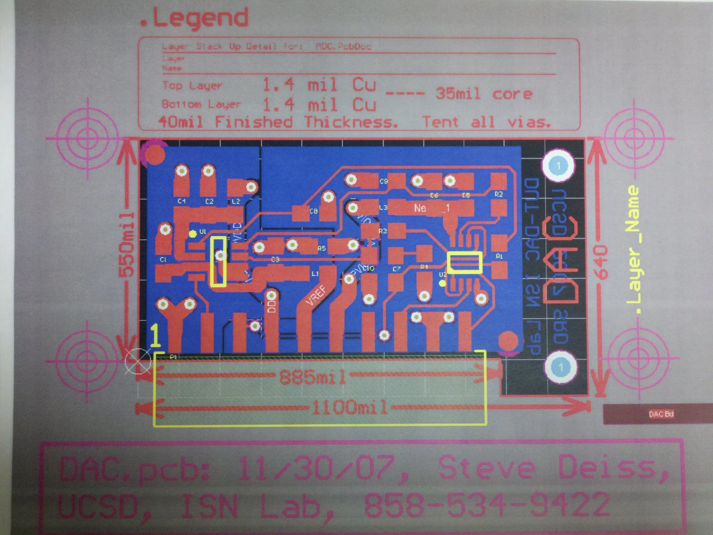
Likewise, this tiny board would do digital to analog conversion for DUT analog input pins. Not long after completion of this design, funding for my position came up short. I built and assembled this 3 board system, but without continued funding for me to finish testing, coding the FPGAs, and help graduate student users, it was not used very much, if at all.
_________________________
2011-12: For a period of a few years I did what one might call odd jobs at the university. After searching for a while I joined a neuroimaging group. There I worked on parameterizing some C++ code that simulates thalamocortical activity based upon settings of cellular currents. It was written by Maxim Bazhenov, our collaborator. The parameterizaiton allowed us to do simulation experiments led by Rachel Mac McCully working on her PhD under Prof. Eric Halgren. I wrote further Matlab code that would allow us to visualize the spiking activity and display cortical up and down states, K complexes, spindles, and related activity in the EEGs being taken from live humans. We collaborated with Sid Cash’s who worked with epileptic patients. He used implanted arrays on the cortex (aka ECOG) of patients being analyzed prior to surgery for removal of the seizure locus. This takes several days and with patient consent it is possible for the patient to do modest experimental tasks while measuring their EEG inside the skull. To make it possible to run many simulations and in parallel, I created a cluster job submission and tracking system so that Rachel could feed many jobs with the parameters set, and then go pick up the results to visualize as they completed. As another part of the project I created a simplified MEG/EEG/MRI signal processing pipeline combining tools that were around the lab in code libraries. This was arranged so that a user could specifiy the type of analysis to be done, the data set to run on, and various control parameters ahead of time. Then the proper tools would be run in the proper sequence to analyze the dataset and plot results. This was a nice refresh on software and Linux for me after years of hardware design with Windows. All this work together resulted in an important paper for Rachel and her thesis. Soon after, the PI lost a chunk of his funding, and I was lowest seniority for coverage having been there just over a year.
_________________________
2013-2015: So the next odd job that came along was to help in the Swanson Lab where they were trying to make hardware design really simple for CSE students. This was by allowing them to hook up icons on a screen like lego blocks which corresponded to little hardware subsystems. They could simulate what it would do, and then they could submit it for fabrication. I designed a couple of small Arduino board knock-offs to support this project, and I also experimented with interfacng to one of the Qualcomm Snapdragon boards. However, much of my time was also spent testing nonvolatile memory units to ensure that they were securely erased. That was a significant learning curve for me using Linux, CENTOS, and UCSD networking, having come from a Windows user background. The result was a large BASH script to automate the process and produce detailed reports. As funding for this wound down, things started opening back up in the Cauwenberghs lab and finally became full time again. Such was my serial orphan experience at UCSD. The next ISNL project was to troubleshoot the latest IFAT board system below.
_________________________

2015-16: ‘IFAT’ stands for Integrated Fire Array Transceiver. It is a simple model of a neuron that integrates multiple received spike-like inputs as an integrated circuit, and produces its own spike-like output to trasnmit when a threshold is crossed and other optional conditions are met. There have been prior generations of IFAT designed at UCSD ISNL (see T. Yu for example). This board held a chip designed by Jongkil Park emulating 64K analog neurons coupled by a hierarchical arrangment of addresss-event busses called HiAER. It was controlled by an FPGA programmed by Bruno Pedroni. My job was to improve the PCB layout and add SDRAM and then get it to work better. It had unusual anaog problems that mystified us all. With some brute force tricks (frequent resets) we were able to get it to generate spikes and act like a neural network. More urgent projects left this IFAT instance set aside indefinitely (until the next iteration) since the designer had long since graduated.

2017-18: Working with Gert and then graduate student Akshay Paul I created this version of a 32 channel ADC board for EEG data aquisition connected in turn to a transition board that interfaced to a PC. This design was a variation on a public domain design though with very careful layout for noise and impedance control and high speed acquisition. To this we could attach EEG electrode arrays with the ultimate goal to acquire EEG from an in-ear device. It became a platform for testing several iterations if in-ear device prototypes. Akshay and his team later did a very capable new version of this of their own.
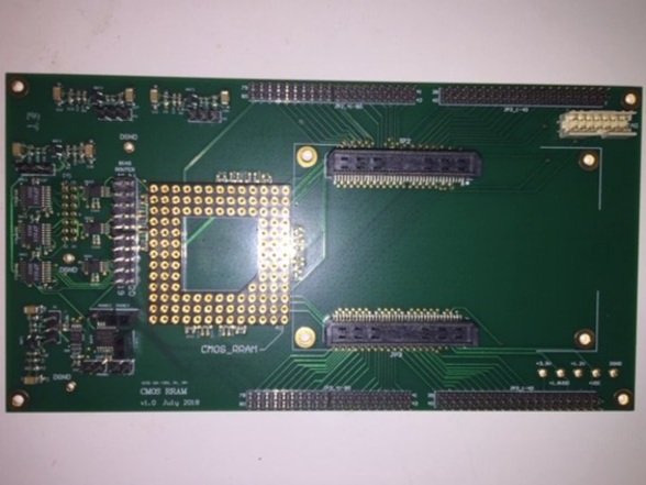
2018: This design was one of a series used in the lab for testing new ICs. Each variant had its own power supplies, socket, jumpers, and analog circuits on the left. On the right was a pair of daughterboard connectors and breakout header strips to allow probing all the signals on the daughterboard. The daughterboard itself was one of the generations of Opal Kelly, such as the XM6310 with FPGA on board and interface to a PC for control. The Opal Kelly could be programmed to generate test patterns for the ‘DUT.’ If memory serves me, Raj Kubendrum and/or Siddharth Joshi did the first of these with just a little advice. The approach became popular. I did the second for Hesham Mustafa, and there may have been a third done for Weier Wan's amazing RRAM chip.
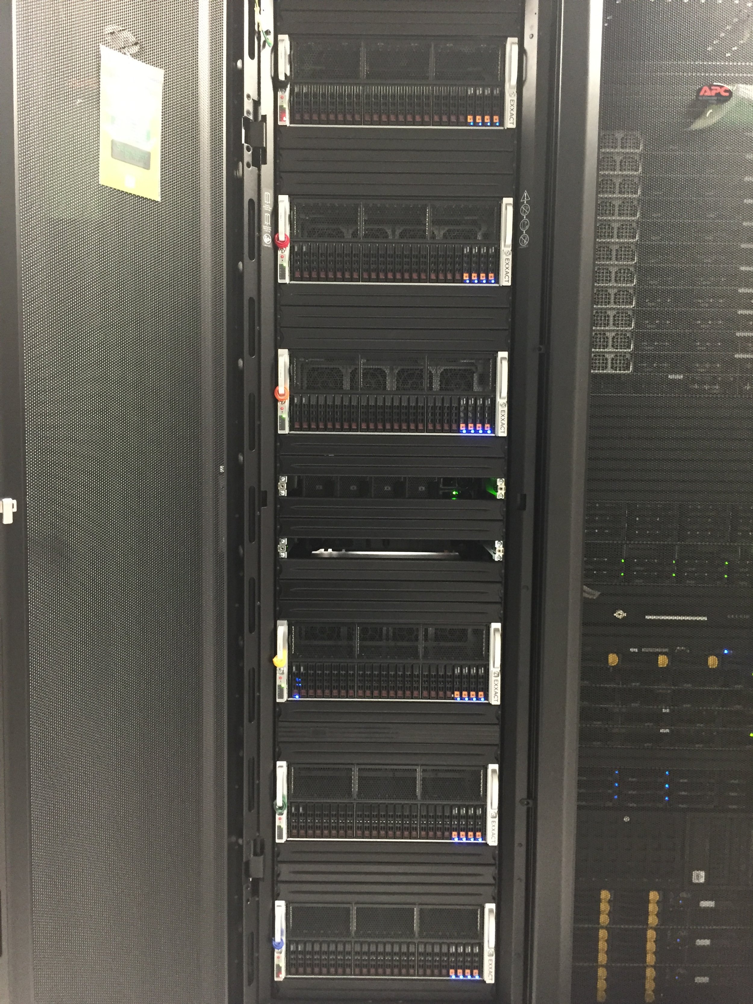
2018-202X: This is our most recent hardware system for neuromorphic system emulation, and my last design before retirement. It is all digital and housed in the San Diego Supercomputer Center. Our system is one of hundreds of ~8 foot high racks of equipment there. Our system provides emulation tools through the Neuroscience Gateway. This ‘NSG’ provides access to a wide variety of neuroscience and neuroengineering tools through its web portal. We call our system HiAER-Spike to reflect its focus on spiking neuron models and the system’s architecture involving a hierarchy of networks passing around event representations packets in parallel.
The system consists of 6 powerful compute servers from EXXACT Corp. (an OEM for Supermicro) with dual EPYC 32 core AMD CPUs, a TB of SDRAM and 25 TB of enterprize grade SSD. One is a system head node and Neuroscience Gateway job control interface. The other 5 contain 8 FPGA boards each with very large I/O bandwidth for spikes and with a Xilinx XCVU37P FPGA. The Verilog code is tailored to make the most of the FPGA’s high bandwidth memory. The memory for each FPGA is 8 GB SDRAM and has over 450GBps peak bandwidth. Each board has an aggregate bidirectional I/0 bandwidth of 500Gbps for communicating spikes as we configure it. All together the system should max out to emulate nearly 160 million neurons and up to 40 billion synapses depending on DRAM partitioning. We used Alpha Data ADM-PCIE-9h7 FPGA boards and Samtec ‘Firefly’ high speed interconnects. Many thanks to go to Tom Whitlock and Kevin Roth at Alpha Data for FPGA and software support, and to Roger Miller at Samtec for Firefly support on this. Also, thanks to EXXACT Corp. staff for all the handholding I required for this, my first, server rack design. We also use an Arista Networks 64 port P4 switch to provide spike communications between servers, and two other switches to provide for control and file sharing. Thanks to Arista for supporting us with hardware for the project. Thank to Western Digital for programming support.
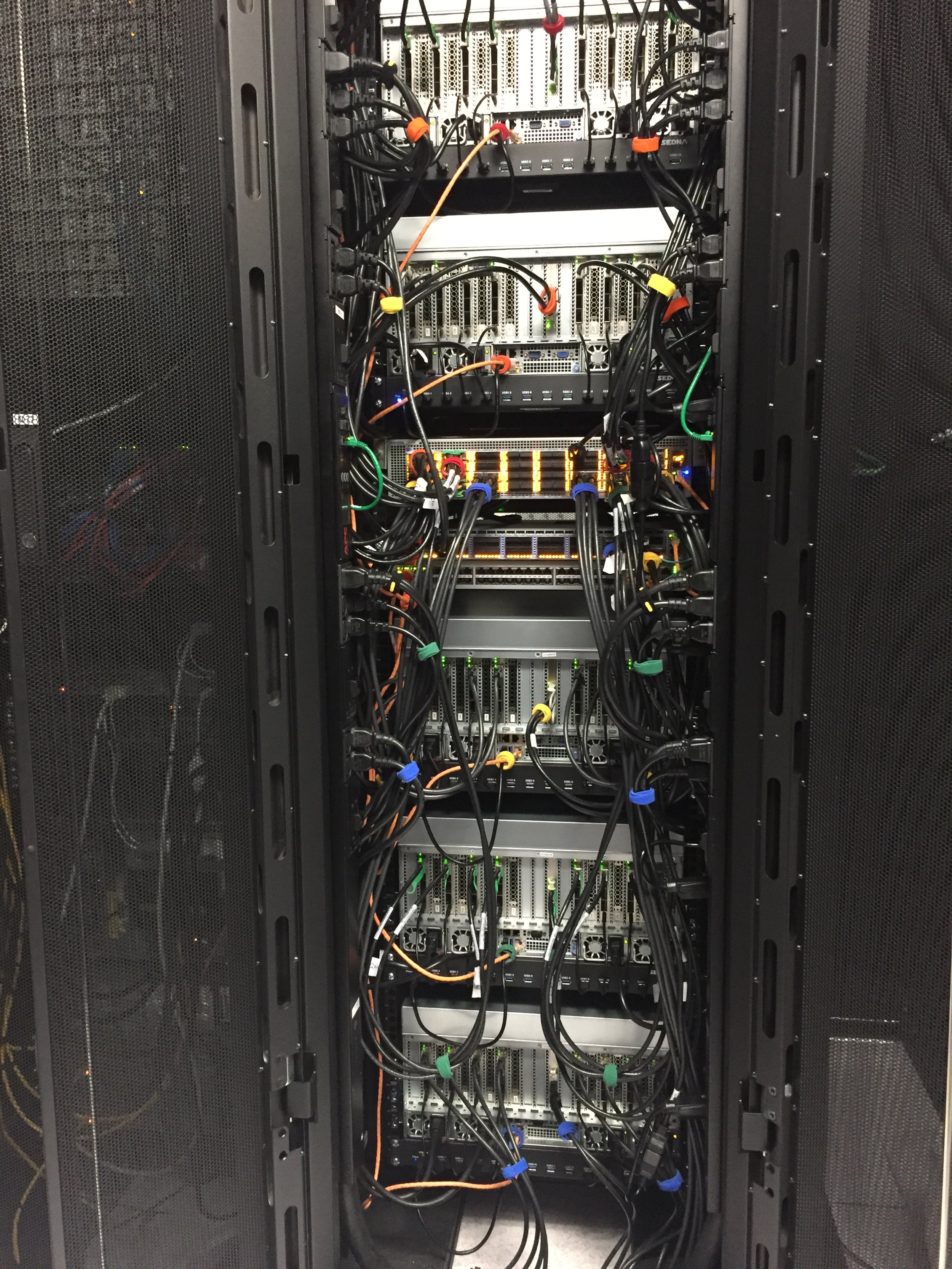
The following photo shows the I/O side of the rack which also includes the 3 Arista switches. One is for 1 Gbps remote server monitor and control. One has 12 100Gbps links for file sharing between servers, and one is the programmable P4 switch that will provide interserver spike distribution at 100Gbps for each of 40 links. Each server from EXXACT Corp. also has 4 redundant 2KW power supplies for reliability.
More details of HiAER-Spike archtecture are to follow in various publications that track development progress. In addition to this hardware system design and construction, the FPGA design and software design were done by a team of about 3 dozen people from our lab or related labs and companies. You can get a sense for the size of the team from any of these publications such as _____. My part was to select, configure, test and install all the equipment and wiring in the rack and do some of the FPGA programming. Many thanks to the entire UCSD ISN HiAER Spike team (including our IT support), SDSC, Western Digital Corp., Arista Networks, Samtec Corp., and not least, Alpha Data Corp. who all helped make this happen . . . and who still keep it happening.
If you have read this far, you can see there were many research projects that receive a grade of incomplete. Nevertheless, I hope you can also see a thread of continuous improvement with positive results.
After retirement I continue to advise the UCSD ISNL group (Cauwenberghs Lab) as an Associate of the UCSD Institute for Neural Computation.